Industrial Components
Photonics Is Becoming the Hidden Compute Bottleneck
As electrical interconnects hit bandwidth and power limits, optical components and their manufacturing capacity become central to compute systems. This is the wafer-to-link map of where the chokepoints sit.
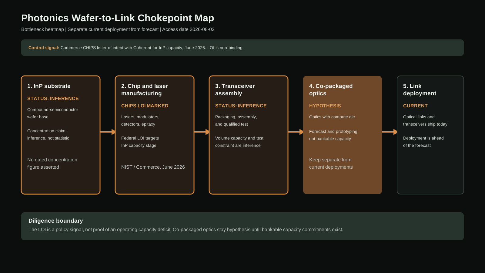
Atomic answer
Compute scaling has a wire problem. Chips get faster, but the electrical links between them hit bandwidth and power limits, and the industry's answer is optical: move data between chips, packages, and racks as light. That shift may make photonics manufacturing capacity a chokepoint in the compute stack; this article does not establish a quantified capacity deficit. The signal is federal and dated: in June 2026, the Commerce CHIPS program announced a letter of intent with Coherent for indium-phosphide (InP) capacity, putting federal capital behind the photonics manufacturing base. The practical distinction: photonics is not one product. It is a manufacturing stack from wafer to link, and the constraint sits in the middle, in InP substrates, laser and detector manufacturing, transceiver assembly, and test equipment. Co-packaged optics are the forecast; the manufacturing capacity that makes them real is the current bottleneck, and the two should never be confused in a diligence memo. The bottleneck operates in Layer 3, Compute & AI Infrastructure: the interconnect layer of the compute stack is where the constraint binds.
Who is this for?
This article is for the compute-architecture founder, the semiconductor allocator, and the data-center planner deciding where optical capacity actually sits.
The decision in front of you: can you separate current optical deployments from co-packaged-optics forecasts, and do you know where the manufacturing capacity sits for each? A project that is real today and a roadmap that is not are different assets, and they deserve different diligence.
Where does it actually bottleneck?
The bottleneck is in Layer 3, Compute & AI Infrastructure, because the constraint sits inside the compute stack's interconnect layer: the links between chips, packages, and racks are the stage that cannot scale. The photonics manufacturing base is the mechanism inside that layer; Layer 1, Materials & Processing, is connected.
Every compute system is a network of compute. The chips compute, and the links between them move the result. For decades the links were electrical, and electrical interconnects scaled comfortably. That stopped being true at the data-center scale of the AI buildout: bandwidth and power per bit became the constraint, and optics became the substitute. The economics are the point, not the physics: optical links move more data per watt and per meter than electrical ones at the lengths the data center needs. The industry is pushing optics ever closer to the chip, from the rack, to the board, to the package, and finally onto the chip itself. Every step down that path increases demand for optical components and for the manufacturing capacity that produces them. Source confidence: Analytical (ecosystem observation, consistent with verified IEEE Spectrum coverage of interconnect and materials limits). Signal strength: Medium.
| Stage | What it is | Where the chokepoint sits | Evidence level | | --- | --- | --- | --- | | Substrate | InP and related compound-semiconductor wafers | Compound-semiconductor wafer capacity is thin and concentrated | Inference | | Chip and laser manufacturing | Lasers, modulators, detectors on photonic integrated circuits | Fabrication and epitaxy capacity; federal LOI targets this stage | Verified (CHIPS LOI) | | Transceiver assembly | Packaging lasers and detectors into pluggable modules | Assembly and test capacity at volume | Inference | | Co-packaged optics | Optical components co-packaged with compute die | Mostly forecast and prototyping; not yet bankable capacity | Hypothesis | | Link deployment | Deploying optics in the network | Deployments are real today; this stage is ahead of the forecasts | Verified (structural) |
The substrate and manufacturing-base concentration claims are inference, not verified concentration statistics: no dated source for the concentration figure was available at the 2026-08-02 cutoff, and it stays labeled as inference. Source confidence: Inference. Signal strength: Medium.
Who controls it?
The federal signal is the cleanest control data point. In June 2026, the Commerce CHIPS program announced a letter of intent with Coherent for indium-phosphide capacity, the compound-semiconductor platform that underlies laser and photonic-component manufacturing. (NIST / Commerce, June 2026, accessed 2026-08-02.) Source confidence: Primary (nist.gov, verified HTTP 200). Signal strength: High.
A letter of intent is non-binding, and the conversion from LOI to award to production capacity is the story, not the announcement itself. The LOI is a policy signal for photonics manufacturing, not proof that a national capacity deficit exists or that new capacity is already operating. Source confidence: Primary for the LOI; Analytical for the read.
The industry side of control is the manufacturing base itself. The deployment side needs assembly and test capacity at volume, and qualified optical test capacity is scarce relative to the transceiver volume the data centers want; that test-equipment chokepoint claim is an inference pending a dated capacity figure. Source confidence: Inference.
Why should founders care?
Three mechanisms, not recommendations.
First, deployments and forecasts are different assets. Deployments are real today: optical links are in the data centers, transceivers are shipping, and the industry's near-term demand is measurable. Forecasts are the future: co-packaged optics, optics integrated onto the compute die, and the extreme-scale versions of the roadmap. The manufacturing-capacity question is different for each. A company selling co-packaged optics is selling a forecast until the capacity is bankable. The single most common error in photonics coverage is conflating the two, and the discipline of this map is to separate them.
Second, the constraint sits in the middle of the stack, not at either end. Substrate capacity is the base: compound-semiconductor wafers are thin and geographically concentrated, and every laser and detector starts as a wafer. The manufacturing stage above it, epitaxy and fabrication, is the stage the federal LOI targets, and it is the stage where capital and yield decide who participates. Read the map from substrate to link and the pattern is the same one the site maps everywhere else: the constraint sits in the manufacturing base, not in the design. Source confidence: Analytical; the concentration claims remain inference-labeled.
Third, the capital question is a manufacturing-base question. Co-packaged optics remain forecast and prototyping, and they stay Hypothesis until bankable capacity commitments exist. The deployment side is where the near-term money is: qualified optical component and test capacity will decide how fast the near-term buildout runs, and it is the manufacturing base, not the roadmap, that deserves the long-term contracts. Source confidence: Hypothesis for co-packaged optics; Analytical for the deployment read.
FAQ
Q: Is photonics really a bottleneck, or a future story? A: Both, and that is the trap. The deployment side is real today: optical links and transceivers are shipping, and assembly and test capacity at volume is the constraint. Co-packaged optics are the future story, and they remain forecast and prototyping. Never confuse the two in a diligence memo. Source confidence: Analytical.
Q: What did the CHIPS letter of intent with Coherent actually commit? A: A letter of intent for indium-phosphide capacity, announced June 2026. It is non-binding, and the conversion from LOI to award to production capacity is the story. The direction is a federal demand signal for the photonics manufacturing base. Source confidence: Primary for the LOI; Analytical for the read.
Q: Where in the stack is the chokepoint? A: In the middle: InP substrates, laser and detector manufacturing, transceiver assembly, and test equipment. Substrate capacity is the base and every laser starts as a wafer; test capacity is scarce relative to transceiver volume. Source confidence: Inference for the concentration claims.
Q: Are compound-semiconductor wafers really concentrated? A: That claim is labeled inference in this piece because no dated concentration source was available at the 2026-08-02 cutoff. Treat it as a hypothesis for navigation, not a verified statistic. Source confidence: Inference.
Q: What should a data-center planner lock in? A: Qualified optical component and test capacity at volume, because that is the deployment-side constraint. The manufacturing base, not the roadmap, deserves the long-term contracts. Source confidence: Analytical.
Q: When do co-packaged optics become bankable? A: When they convert from papers and prototypes into bankable capacity commitments. Until then they are a forecast, and the map keeps them in the Hypothesis column. Source confidence: Hypothesis.
Sources
- Commerce CHIPS letter of intent with Coherent for indium-phosphide capacity: NIST / Commerce (June 2026, accessed 2026-08-02). Primary.
- Interconnect and materials limits driving next-generation compute design: IEEE Spectrum, semiconductors (accessed 2026-08-02). Primary (root).
- CHIPS program context: NIST CHIPS (accessed 2026-08-02). Primary (root).
- Co-packaged optics status (forecast and prototyping): vendor roadmaps and standards, secondary; labeled Hypothesis pending bankable capacity commitments.
- Compute and AI infrastructure context: Sovereign AI Explained (accessed 2026-08-02). Site article.
- Materials and processing bottleneck lens: Materials Bottleneck article (accessed 2026-08-02). Site article.
- Bottleneck Map pillar: Bottleneck Map (accessed 2026-08-02). Site pillar.
Publication cutoff: 2026-08-02.
Methodology
This article follows the Bottleneck Map method. The bottleneck is assigned to Layer 3, Compute & AI Infrastructure, because the constraint sits inside the compute stack's interconnect layer; the photonics manufacturing base is the mechanism, and Layer 1 (Materials & Processing) is connected as the layer where that mechanism binds. Layer 6 (Non-Dilutive Capital) is connected through the CHIPS program.
Every claim carries a source-confidence classification per the editorial standards: Primary where a named, publicly verifiable institutional source is cited inline; Analytical where the claim reflects Stack & State ecosystem observation; Inference where the claim is a strong inference from multiple sources without a dated primary; Hypothesis where the claim is analytical judgment pending verification. The substrate and manufacturing-base concentration claims stay labeled as inference because no dated concentration source was found in this run. Co-packaged optics stay Hypothesis until bankable capacity commitments exist. No specific capacity number is asserted without a dated source, and no URL is invented.
Research cutoff and access date for all sources: 2026-08-02. Corrections: /connect/.
Stack & State is an editorial and ecosystem-intelligence publication. Nothing here is legal, investment, procurement, or compliance advice. Program details change; verify requirements with primary sources and qualified advisors.